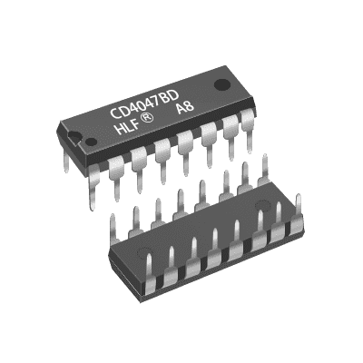
CD4047BD
The CD4047B is able to work in either an unsteady or unsteady mode. It requires an external capacitor to (Between pins 1 and 3) and an external resistance (lead Between feet 2 and 3), to determine the output pulse width in the unsteady mode, and the output frequency in the unsteady mode. Monstable mode is done by entering a high level at the astable pin or atastablePin input of the low level implementation. Output frequency (50% duty cycle) end Q andQIt is determined by the timing elements. The Oscillator oscillator output is twice the frequency of the Q end; a 50% duty cycle is not guaranteed. Unsteady modes include: up along the level or down the level at the-trigger input. The chip can be retrigger ed by synchronizing ascending along the + trigger and retriggering the input. Upper reset end input high level, reset output Q is low level,QHigh-level level.
Features
Wide power supply voltage range: 3.0V to 15V
High immunity: 0.45 VDD()
Low-power consumption, TTL is compatible Special Features
Low power consumption: a special CMOS oscillator configuration
Unistable (single) or unsteady (free-run) work
Actual compensation buffer output
Just one external R and C
Application:
Frequator
Timiming circuit
Delay Application
Enenvelope wave
Frequency-doubling
Frequency-sharing
-
Tel
(86)755-83041584 -
Wechat


